Intel Foundry is sending a clear signal to the semiconductor ecosystem: the era of unpredictable timelines is officially in the rearview mirror. In a media briefing ahead of the 2026 VLSI Symposium, the company provided an early look at its latest manufacturing advancements.
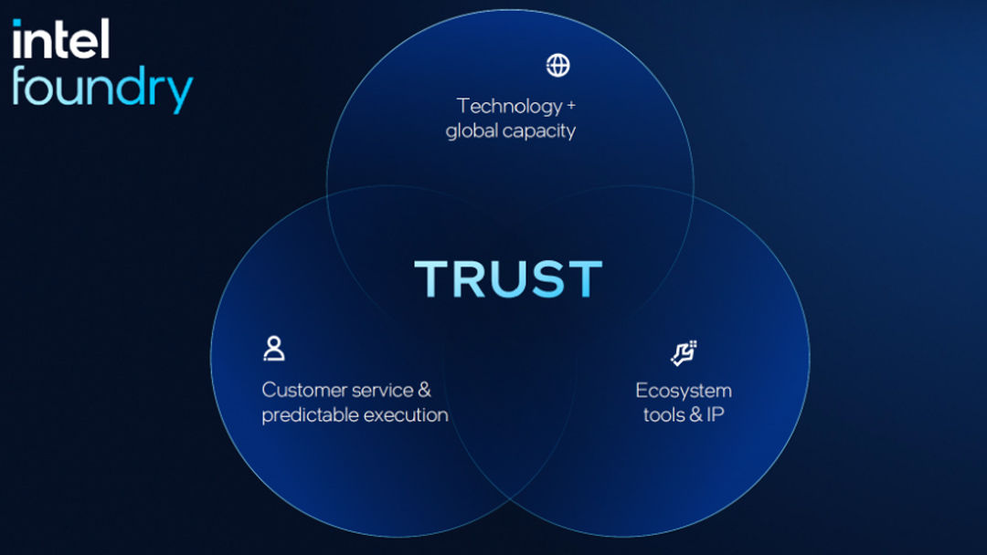
Intel Vice President Chris Auth emphasized that trust is the foundation of their new approach. By meeting strict deadlines and delivering on technical promises, Intel aims to be the go-to partner for companies building the next generation of computers and AI technology.
The Strategic Imperative: Trust and Predictability
Predictability is now the core mission. Tech companies need to know exactly when new manufacturing capabilities will be ready so they can plan their own product launches. Intel is using its latest milestones to prove that its “18A” family of technology is on track for release this year.
The 18A Foundation and the High-Performance Compute Advantage
To meet the massive power needs of AI, Intel has implemented two major design changes that act as the engine for these new chips:
- RibbonFET: Intel's gate-all-around transistor design utilizes four ribbons, providing increased drive current compared to the three-ribbon designs used by competitors.
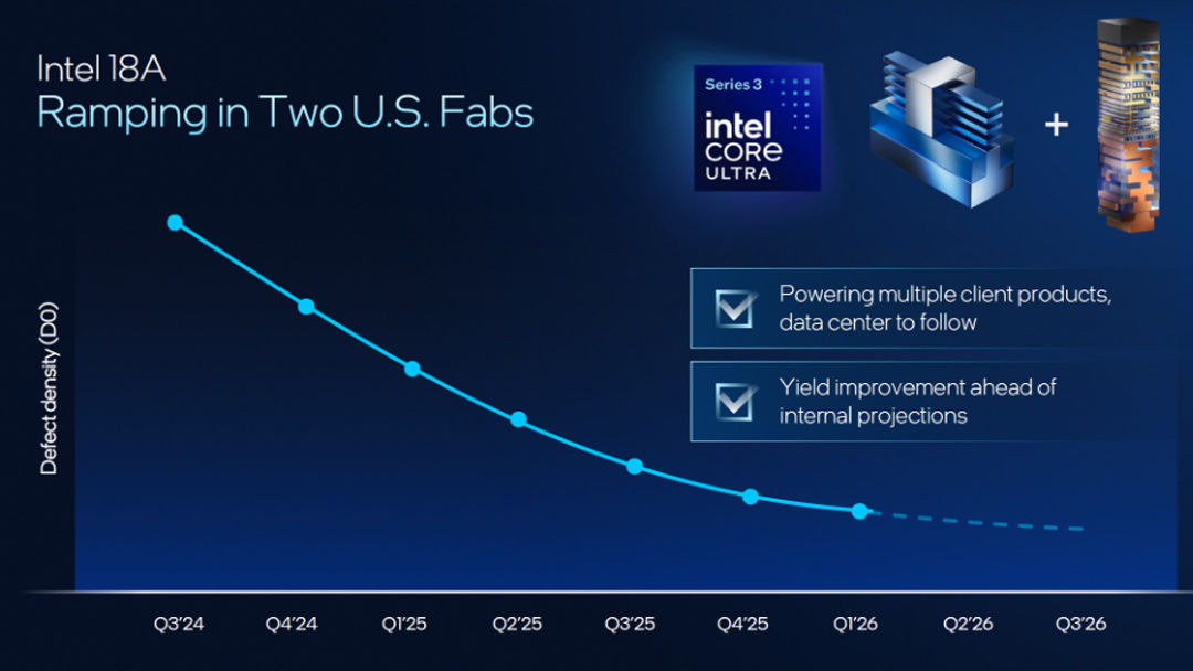
- Backside Power: Traditional chips face a bottleneck as massive power lines and narrow signal lines compete for space. Intel moved the power lines to the backside of the chip, delivering power directly to the transistors and freeing up front-side space to reduce signal interference. This process, introduced with the Panther Lake launch late last year, is currently ramping up with continued improvements in defect density and yield.
In response to competitor claims around superior transistor density based on metrics tailored for mobile devices. Intel's messaging effectively reframes this debate: raw density matters less than performance-per-watt and thermal dissipation in HPC. By utilizing large transistors and 160 cell heights, Intel aims to dominate the high-performance compute and AI accelerator markets where thermal management rules supreme.
Introducing Intel 18A-P: The First Major Enhancement to Intel 18A
The centerpiece of the briefing was the introduction of Intel 18A-P, the first performance enhancement within the Intel 18A family. Designed as a superset, 18A-P adds new features while maintaining full backward compatibility. This compatibility allows clients to design with confidence, knowing they can migrate designs from 18A to 18A-P without adjustments.
Crucially, 18A-P has already entered risk production, meaning Intel has enough confidence in the defect density and yield data to begin manufacturing ahead of full qualification.
Intel 18A-P delivers highly competitive power, performance, and area (PPA) improvements:
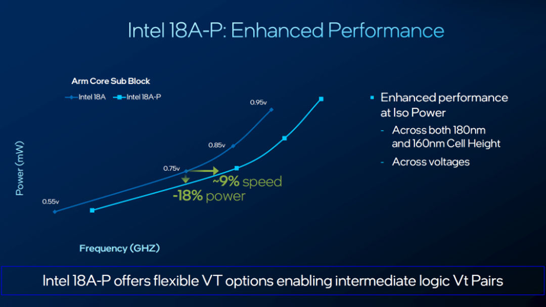
- Power and Performance Gains: 18A-P achieves an 18% reduction in power consumption at constant performance, or a 9% performance increase at constant power compared to 18A.
- Thermal Upgrades: 18A-P introduces a 20% to 40% improvement in thermal resistance. Intel achieved this by reducing the thickness of the thermal handler wafer, utilizing new materials, and deploying thermally-aware EDA tools to route heat effectively.
- Reduced Resistance: Resistance at critical via layers has been reduced by 10% to 30%.
Standardized Benchmarking, Architectural Flexibility, and Tighter Process Control
In demonstrating 18A-P’s capabilities, Intel made the notable choice to use an ARM core subblock as its primary test vehicle. While this might raise questions about Intel’s traditional role as the x86 flag bearer, Auth clarified that the decision was strictly about standardizing metrics for clear, “apples-to-apples” industry comparisons against competitor foundries. Auth firmly dispelled any notion of an x86 deemphasis, assuring that 18A and 18A-P are heavily designed for x86 architecture, which remains one of their largest customer segments.
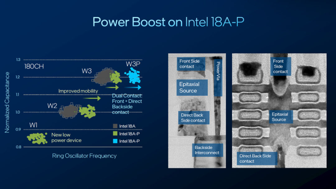
To give all designers more control, whether they are building standard ARM or custom x86 silicon, Intel 18A-P significantly expands available device offerings:
- New Device Widths: A W1 cell with highly narrow diffusion is available for ultra-low toggling power, alongside a new 1.5 width for the 180 cell height.
- Power Boost (W3P): This new dual-contact low-resistance cell uses direct backside contacts to relieve funneling bottlenecks. While it demands more power when active, it provides vital high performance for critical circuit paths without taking up additional area.
- Extended Voltage Control: A fifth logic threshold voltage (VT) pair has been introduced specifically between the Ultra-Low Threshold Voltage (ULVT) and Low Threshold Voltage (LVT) spectrum to maximize design flexibility.
To achieve these results, Intel implemented significant structural changes at the transistor level, bypassing historical bottlenecking while mitigating the intense heat generated by high-compute workloads.
Looking Ahead
Looking further out, Intel is researching even more advanced methods to keep its lead. This includes stacking components vertically to save space, using new materials like ruthenium for even smaller wiring, and integrating power regulation directly onto the chip to maximize efficiency for data centers and AI workloads. By hitting these milestones on schedule and proving the efficiency of the 18A-P process, Intel is positioning itself as the most reliable manufacturing partner for the AI era. The focus remains clear: delivering high-performance, cool-running technology exactly when the market needs it.