I have always wondered how these highly sophisticated and intricate microprocessors, which house tens of billions of transistors, are actually manufactured. During the Intel Tech Tour to Arizona earlier this month, I had the extraordinary experience of seeing where the chips I’ve spent my life reviewing truly begin their journey. And I could not have been luckier. I had the opportunity to visit Intel’s Fab 52 facility at the company’s Ocotillo campus in Chandler, Arizona, where the world’s most advanced processors are manufactured at scale using Intel’s 18A process technology. This is the process that will power Intel’s upcoming Panther Lake and Clearwater Forest series of system-of-chips-based processors, which, for the first time, will combine RibbonFET and PowerVia technologies to deliver class-leading efficiency and performance potentially. You can read my deep dive on Panther Lake here for more on what makes it a significant step in Intel’s roadmap.
A Childhood Dream Come True
For more than twenty years, I have spent my days surrounded by processors, testing them, reviewing them, and often pointing out what they got right or wrong. My world has always been on the other side of the finished product: performance numbers, benchmarks, and charts. But nothing in all those years prepared me for what it felt like to step inside Intel’s Fab 52 in Chandler, Arizona. It is one thing to read about how chips are made. It is something completely different to see it happen right in front of you.
Fab 52 sits within Intel’s Ocotillo campus, a massive complex in the middle of the Arizona desert. Backed by a 32 billion dollar investment, it is one of the most advanced semiconductor manufacturing sites in the world. This is where Intel produces chips using its latest 18A manufacturing process, the company’s latest and most advanced technology. It is also a crucial component of a broader initiative to expand semiconductor manufacturing in the United States. Walking through the facility, it becomes clear why Intel considers this place more than just a factory. It represents a convergence of scale, precision, and years of engineering expertise.
Preparing to Step Inside: The Bunny Suit
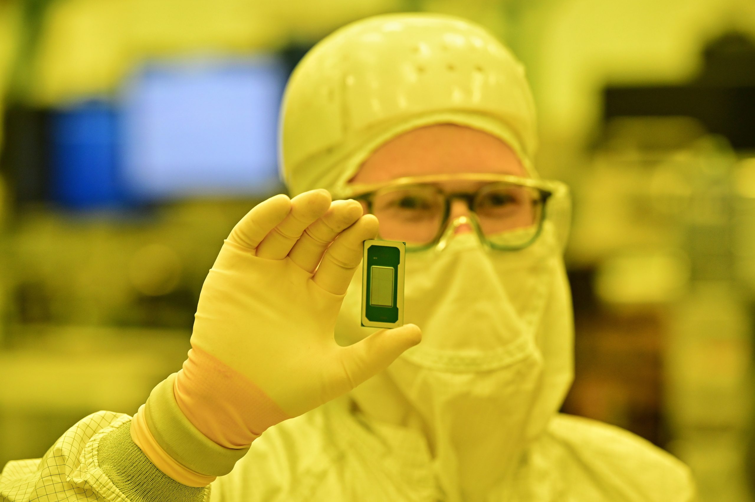
Before entering, the preparation process itself was an experience. Every personal item and gadget, from phones to even pens and notepads, had to be left behind. We were provided with special notepads and pens for use within the facility. We were also instructed to refrain from wearing any perfumes, lotions, or scented products, as even trace vapours could interfere with the highly controlled environment. Then came the cleanroom attire, known as the “bunny suit.” Putting it on was a slow and careful process, with trained staff checking every seam and closure to ensure nothing from us could contaminate the pristinely clean and sanitized surroundings. Even beards and stubble had to be fully covered with protective masks. We were also instructed not to mention or identify any of the equipment manufacturers inside the fab, a reminder of how closely guarded everything there was. By the time I was ready, I felt like I was about to step into a whole new world. And a whole new world it was!
Inside the Fab: A World of Precision and Control
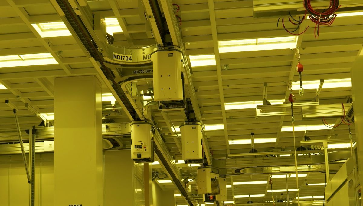
Inside, the cleanroom was unlike anything I had ever seen. The first thing I noticed was the sound: a steady, constant hum from machines running all around. One of the most striking technical features inside was the Automated Handling and Material System (AHMS), an intricate network that managed the movement of sealed containers called FOUPs, short for Front Opening Unified Pods, along ceiling-mounted tracks. Overhead, the system’s robotic carriers glided with precision, transporting FOUPs between different departments and processing tools, ensuring that each batch of silicon wafers remained isolated entirely from contamination or human contact. The coordination was incredible, almost too perfect at times, like something out of a science fiction movie where humans and robots work together in quiet harmony. For a moment, I wondered if these machines ever made mistakes or came close to colliding as they crossed paths, but I did not ask. My mind was too busy trying to take in the scale of everything around me.
It was a guided and tightly controlled tour, but I did find myself wondering what other parts of the fab looked like. The thought of sneaking off to explore did cross my mind, but it did not last long; clearly, it was not an option in a place like this. The air inside Fab 52 felt unusually clean. Coming from Delhi, where clean air is often a luxury, it took me a few minutes to adjust. It is filtered and recirculated hundreds of times every hour to remove even the smallest dust particles. It feels still, light and dry, besides being incredibly clean and easy to breathe.
As we moved deeper into the facility, another fascinating section came into view: lithography. When we entered the area, the lighting changed to a soft yellow colour. This lighting protects the light-sensitive materials used to etch circuit patterns onto wafers. It is here that some of the most advanced machines in the world operate, the EUV lithography systems that use light to print transistors on silicon. Watching them work was fascinating. These machines use laser-produced plasma to carve patterns that are only a few atoms wide. The level of accuracy is difficult to grasp until you see it up close.
As the tour continued, I began to understand the scale of what happens here. The floors are reinforced to absorb vibration. The air, temperature, and humidity are kept stable to the smallest margin. Even the slightest environmental change can affect production.
A Shift in Perspective
Being inside Fab 52 made me think differently about processors. I have spent years judging them by performance and efficiency numbers, often without considering the amount of work that goes into making them. Those 30-odd minutes of seeing the process up close changed that. Each chip represents years of research, the work of thousands of people, and an enormous amount of precision and care. During an earlier chat with Intel’s Daniel Rogers, he told me that Intel 18A was the “magic sauce” behind Panther Lake, the foundation that would define Intel’s next-generation compute platforms. Standing inside the very place where that technology is taking shape made that statement resonate in a way it never had before.
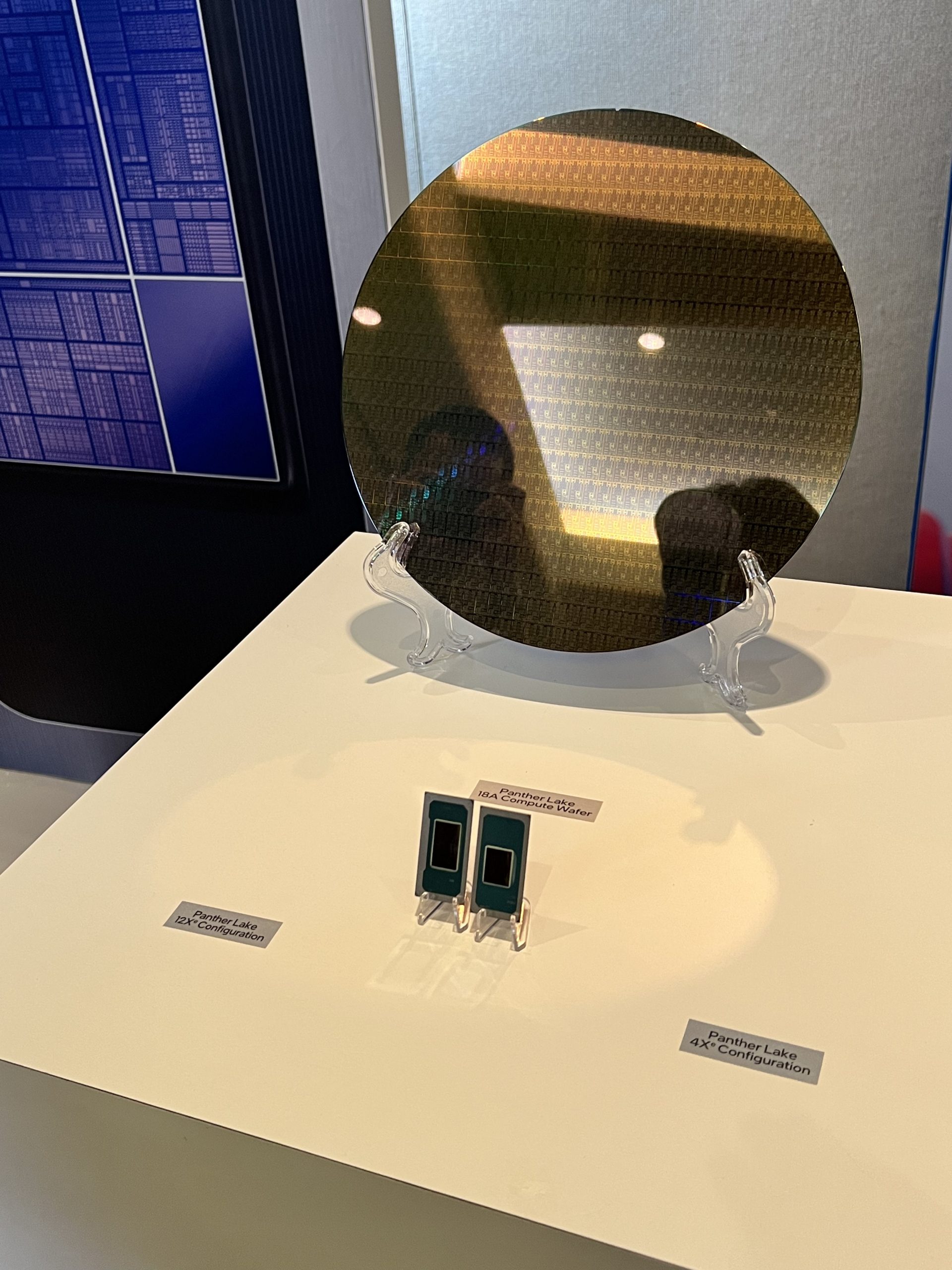
When the visit ended and I stepped out of the cleanroom, I felt a deep respect for the scale and precision of what I had seen. The Fab 52 tour gave me the perspective that creating processors is far more complex and demanding than performance charts or benchmarks can convey. As I left the site, I was reminded that progress in this industry is not just about performance or speed, but about persistence, vision and precision.